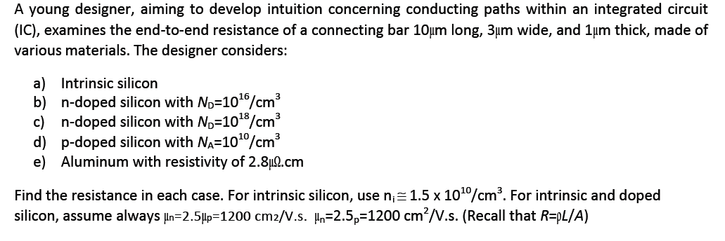
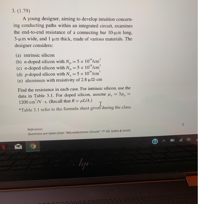
British designer Matthew Blick devised an innovative package for Edward Bulmer. 36 A young designer aiming to develop intuition concern- ing conducting paths within an integrated circuit examines the end-to-end resistance of a connecting bar 10-u m long 3-um wide and 1 um thick made of various materials.

Top Digital Commerce Company San Diego Ca Application Development Development Best Seo Company
People not technology are the drivers of innovation so an essential part of the process involves stepping into the users shoes and building genuine empathy for your target audience.
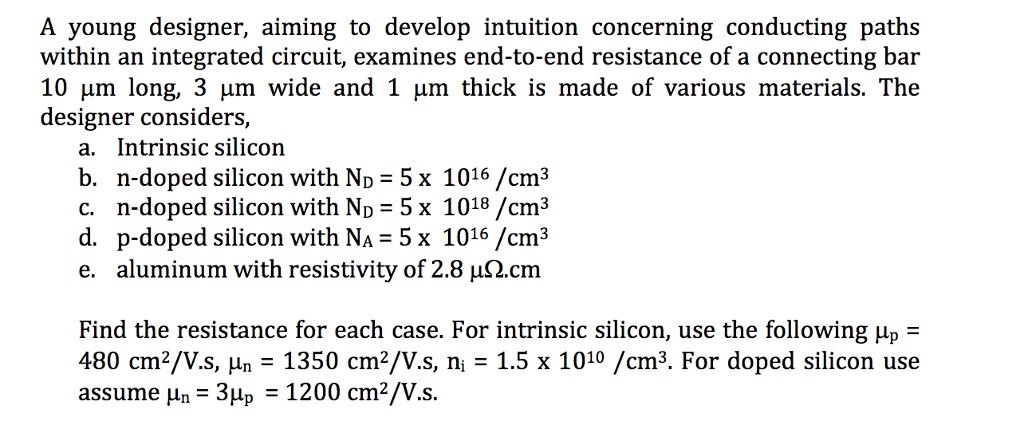
. A young designer aiming to develop intuition concerning conducting paths within an integrated circuit examines the end-to-end resistance of a connecting bar 10 μm long 3 μm wide and 1 μm thick made of various materials. Inspire Influence and Inform. It will be important to develop provide and make the most of existing user-friendly accessible tools for example Youthpass Europass that can enhance the ability of non-formal education workers and youth workers to offer activities that promote innovation and creativity in young people and make young people aware of the skills gained through.
For intrinsic silicon My. In this post we present 17 steps to help improve your architectural design process and concept development that can be implemented straightway. Design thinking is all about finding solutions that respond to human needs and user feedback.
A intrinsic silicon b n-doped silicon with ND 1016 cm3 c n-doped silicon with ND 1018 cm3. N-doped silicon with ND -5 x 1016 cm3 n-doped silicon with ND 5 x 1018 cm3 d. A intrinsic silicon b n-doped silicon with ND 1016 cm3.
The designer considers a. A intrinsic silicon b n-doped silicon with N 5 10cm c n-doped silicon with N 5 x 108cm d p. You can also make a list of creative endeavors and set up individual steps to get there.
A young designer aiming to develop intuition con cerming conducting paths within an integrated circuit examines the end-to-end resistance of a connecting bar 10 μ m long 3 μ m wide and 1 μ m thick made of various materials. A n-doped silicon with ND 1018 cm³ b p-doped silicon with NA 1016 cm³. A young designer aiming to develop intuition concerning conducting paths within an integrated circuit IC examines the end-to-end resistance of a connecting bar 10 mu m long 3 mu m wide and 1 mu m thick made of various materials.
Made of materials. A Video Series Highlighting Young Peoples Role in Positive Youth Development Programs This grant supported the creation of a video series featuring the perspectives and experiences of young people in three countries across Africa and South Asia that address the benefits impacts best. Pots of Paint which is almost 100 compostable.
A young designer aiming to develop intuition concerning conducting paths within an integrated circuit calculate the end-to-end resistance of a connecting bar 10 μm long 3 μm wide and 1 μm thick made of various materials. You can develop it by setting up a new schedulediscipline. Try drawing or writing with your non-dominant hand for 5-10 minutes daily.
A Intrinsic silicon b n-doped silicon with ND1016cm3 c n-doped silicon with. A young designer aiming to develop intuition concerning conducting paths within an integrated circuit calculate the end-to-end resistance of a connecting bar 10 μm long 3 μm wide and 1 μm thick made of various materials. Combined with a growing pressure on corporations to develop more eco-friendly products there are now new opportunities for designers to really push the boundaries with sustainable packaging design.
A young designer aiming to develop intuition concerning conducting paths within an integrated circuit determine the end-to-end resistance of a connecting bar 10um long 3um wide and 1um thick made of various materials. A young designer aiming to develop intuition concerning conducting paths within an integrated circuit determine the end-to-end resistance of a connecting bar 10um long 3um wide and 1um thick made of various materials. Young designer aiming to develop intuition concerning conducting paths within an integrated circuit examines the end-to-end resistance of a connecting bar 10 μmlong 3 μm and 1 μm thick made of various materials.
540- 730 pm Question. A n-doped silicon with ND 1018 cm³ b p-doped silicon with NA 1016 cm³. 36 A young designer aiming to develop intuition con- cerning conducting paths within an integrated circuit exam- ines the end-to-end resistance of a connecting bar 10 µm long 3 um wide and 1 µm thick made of various materials.
Young designer aiming to develop intuition concerning conducting paths within an integrated circuit examines the end-to-end resistance of a connecting bar 10 micrometer long 3 micrometer wide and 1 micrometer thick made of various materials. A young designer aiming to develop intuition concerning conductingpaths within an integrated circuit examines the end-to-endresistance of a connecting bar 10μm long 3μm wide and1μm thick made of various materials. User interface UI design is the process designers use to build interfaces in software or computerized devices focusing on looks.
A young designer aiming to develop intuition concerning conducting paths within an integrated circuit examines the end-to- end resistance of a connecting bar 10 μm long 3 μm wide and 1 μm thick made of n-doped silicon material. Find the resistance of the bar if N D 10 16 cm 3 For doped silicon assume μ n 3 μ p 1200 cm 2. A young designer aiming to develop intuition concerning conducting paths within an integrated circuit examines end-to-end resistance of a connecting bar 10 μm long 3 μm wide and 1 μm thick is made of various materials.
Surround yourself with different settings positive friends and nature. Some of which we have used as students and others we have developed and discovered over time as design architects. Intrinsic silicon n-doped silicon with ND 5 x 1016cm3 n-doped silicon with ND 5 x 10¹⁸.
A young designer aiming to develop intuition concerning conducting paths within an integrated circuit examines the end-to-end resistance of a connecting bar 10-mum long 3-mum wide and 1 mum thick made of various materials. A young designer aiming to develop intuition concerning conducting paths within an integrated circuit examines the end-to-end resistance of a connecting bar 10-μm long 3-μm wide and 1 μm thick made of various materials. A n-doped silicon withND1018cm3 b p-doped silicon withNA1016cm3.

Sample Resume For Internship Getting An Internship In College Seems Like A No Brainer Simply Good Objective For Resume Internship Resume Resume Objective

Rose Design On Instagram Minimalistic Logo Design For Modest Street The Modest Street Is A Streetwear Minimalist Logo Minimalist Logo Design Initials Logo
Solved A Young Designer Aiming To Develop Intuition Chegg Com
Solved A Young Designer Aiming To Develop Intuition Chegg Com

Solved 3 6 A Young Designer Aiming To Develop Intuition Chegg Com

Solved 3 1 79 A Young Designer Aiming To Develop Chegg Com

Solved A Young Designer Aiming To Develop Intuition Chegg Com
Solved 3 1 79 A Young Designer Aiming To Develop Chegg Com
0 comments
Post a Comment